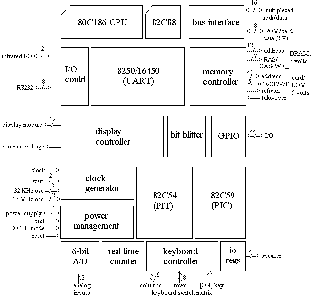
The following is a simplified block diagram of the palmtop IC chip.
Hornet Pin Out
PIN          #    TYPE   SUPPLY   DESCRIPTION
==========================================================================================
Power Supply:
------------------------------------------------------------------------------------------
VCC          5    I      -        Power Supply: 0 to 5.5 Volts
------------------------------------------------------------------------------------------
VDD          5    P      -        Power Supply: 3.0 to 5.5 Volts
------------------------------------------------------------------------------------------
VDDP         6    P      -        Pad Power Supply: 3.0 to 5.5 Volts
------------------------------------------------------------------------------------------
GND          10   I      -        Ground: 0 Volts
------------------------------------------------------------------------------------------
AVDD         1    I      -        Analog Power Supply: 3.0 to 5.5 Volts
------------------------------------------------------------------------------------------
System RAM Interface:
------------------------------------------------------------------------------------------
AD[0:15]     16   I/O    VDD      Multiplexed address/data lines, data lines for RAM.
------------------------------------------------------------------------------------------
CA[0:11]     12   O      VDD      Row/Column Address lines for RAM
------------------------------------------------------------------------------------------
NWE          1    O      VDD      Write Enable; active low
------------------------------------------------------------------------------------------
NRAS[0:3]    4    I/O    VDD      RAS outputs to support 4 RAMs; active low
------------------------------------------------------------------------------------------
NUCAS        1    O      VDD      Upper byte CAS output; active low
------------------------------------------------------------------------------------------
NLCAS        1    O      VDD      Lower byte CAS output; active low
------------------------------------------------------------------------------------------
Note: The RAM NOE pin is tied to GND.

Card/ROM Interface:
------------------------------------------------------------------------------------------
MD[0:7]      8    I/O    VCC      5-Volt data lines
------------------------------------------------------------------------------------------
MA[0:25]     26   O      VCC      5-Volt address
------------------------------------------------------------------------------------------
NCWE         1    O      VCC      Card Write enable; active low
------------------------------------------------------------------------------------------
NRCE         1    O      VCC      ROM chip enable; active low
------------------------------------------------------------------------------------------
NCS[0:1]     2    O      VCC      Active low card selects for 2 cards (Byte
                                  access allows card -CE2 to be tied high.)
------------------------------------------------------------------------------------------
NOE          1    O      VCC      Output enable; active low.
------------------------------------------------------------------------------------------
NCWAIT[0:1]  2    I      VCC      Card Wait signal used to extend
------------------------------------------------------------------------------------------
                                  bus cycle; active low
------------------------------------------------------------------------------------------
NTKO         1    I      VCC      Take Over; If NTKO is shorted to ground by a plug-in
                                  card, all system ROM accesses (NRCE) will be
                                  redirected to NCS[0].
------------------------------------------------------------------------------------------
LCD Module Interface:
------------------------------------------------------------------------------------------
YD (FRM)     1    I/O    VDD      Data for row driver
------------------------------------------------------------------------------------------
LOAD (CL1)   1    O      VDD      Parallel load pulse
------------------------------------------------------------------------------------------
DF (FI)      1    O      VDD      Frame inversion signal
------------------------------------------------------------------------------------------
CP (CL2)     1    O      VDD      Clock pulse; Data is shifted on the
                                  fall of this signal.
------------------------------------------------------------------------------------------
DD[0:7]      8    O      VDD      Data to display column drivers
------------------------------------------------------------------------------------------
Keyboard:
------------------------------------------------------------------------------------------
KB[0:21]     22   I/O    VDD      Keyboard I/O
------------------------------------------------------------------------------------------
KBI[22:23]   2    I      VDD      Dedicated keyboard input
------------------------------------------------------------------------------------------
ON           1    I      VDD      ON key input
------------------------------------------------------------------------------------------
Serial Port:
------------------------------------------------------------------------------------------
RX           1    I      VDD      Serial in
------------------------------------------------------------------------------------------
TX           1    O      VDD      Serial out
------------------------------------------------------------------------------------------
NRI          1    I      VDD      Ring Indicator
------------------------------------------------------------------------------------------
NCTS         1    I      VDD      Clear To Send
------------------------------------------------------------------------------------------
NDSR         1    I      VDD      Data Set Ready
------------------------------------------------------------------------------------------
NDCD         1    I      VDD      Data Carrier Detect
------------------------------------------------------------------------------------------
NDTR         1    O      VDD      Data Terminal Ready
------------------------------------------------------------------------------------------
NRTS         1    O      VDD      Request To Send
------------------------------------------------------------------------------------------
Power Supply Interface:
------------------------------------------------------------------------------------------
VDDOK        1    I      VDD      Vdd OK input from external power supply
------------------------------------------------------------------------------------------
VCCOK        1    I      VCC      Vcc OK input from external power supply
------------------------------------------------------------------------------------------
BUP          1    O      VDD      Backup; driven high to select backup mode
------------------------------------------------------------------------------------------
SON          1    O      VDD      System on; driven high in run and light sleep
------------------------------------------------------------------------------------------
ADC[0:2]     3    I      AVDD     A/D inputs (main batteries, backup battery, and
                                  reference) The analog input range is from
                                  1.57V to VDD.
------------------------------------------------------------------------------------------
Emulation/Test:
------------------------------------------------------------------------------------------
NTEST        1    I      VDD      Test mode input; pulled low to force the part into
                                  test mode
------------------------------------------------------------------------------------------
XCPU         1    I      VDD      External CPU mode input (disables internal CPU and
                                  reconfigures the GPIO pads for an external CPU
                                  interface)
------------------------------------------------------------------------------------------
Other:
------------------------------------------------------------------------------------------
GPIO[0:7]    8    I/O    VDD      General Purpose I/O pins: These signals are used to
                                  interface to software controlled functions in the
                                  PCMCIA card port, the display module, and the power
                                  supply. They can be individually configured as input,
                                  output, or as control output signals such as IOR or
                                  IOW. In XCPU mode, these pins provide the interface
                                  for the external CPU.
------------------------------------------------------------------------------------------
GPIO[8:26]   19   I/O    VCC
------------------------------------------------------------------------------------------
SPK[0]       1    O      VCC      Differential speaker driver pin
------------------------------------------------------------------------------------------
SPK[1]       1    O      VDD      Differential speaker driver pin
------------------------------------------------------------------------------------------
CCV          1    I/O    VDD      Contrast Control voltage; 5-bit D/A output
------------------------------------------------------------------------------------------
IRO          1    O      VCC      LED output driver
------------------------------------------------------------------------------------------
IRI          1    I      VCC      Infrared input sensor
------------------------------------------------------------------------------------------
HXI, HXO     2    I/O    VDD      21.477272 MHz quartz crystal connections
------------------------------------------------------------------------------------------
LXI, LXO     2    I/O    VDD      32.768 KHz quartz crystal connections
------------------------------------------------------------------------------------------
NRES         1    I      VDD      Reset; active low
------------------------------------------------------------------------------------------
TOTAL: 195 + 13 no connects = 208-pin package
In the palmtop product, the GPIO[0:26] pins are allocated as follows:
GPIO  SUPPLY  ALIAS      TYPE  DESCRIPTION
==========================================================================================
0     VDD     IRON3      O     3 Volt IR power on; driven high to enable pullup on IRI
------------------------------------------------------------------------------------------
1     VDD     DVEN       O     Display voltage enable; driven high to turn on display
                               high voltage
------------------------------------------------------------------------------------------
2     VDD     reserved   O     VPPON for second card
------------------------------------------------------------------------------------------
3     VDD     VPPON      O     Programming voltage on; driven high to allow programming
                               of FLASH
------------------------------------------------------------------------------------------
4     VDD     NREFON     O     Reference voltage on; active low
------------------------------------------------------------------------------------------
5     VDD     PON        O     Serial port on; driven high to turn on power to serial
                               driver/receiver chip
------------------------------------------------------------------------------------------
6     VDD     NBVD1      I     Inverted Battery Voltage Detect 1 from card;
                               interrupt/wakeup capable
------------------------------------------------------------------------------------------
7     VDD     NOAC       I     Indicates that AC adapter is not plugged in; interrupt
                               capable
------------------------------------------------------------------------------------------
8     VCC     NCD1       I     Card detect input 1 from card; NMI interrupt
------------------------------------------------------------------------------------------
9     VCC     reserved   I     Card detect input from second card; NMI interrupt
------------------------------------------------------------------------------------------
10    VCC     ECHG       I/O   Enable charge; resistively driven high to enable charging
                               circuit; will be driven low externally if battery
                               overvoltage occurs
------------------------------------------------------------------------------------------
11    VCC     reserved   I     Battery Voltage Detect 1 from second card; interrupt
                               capable
------------------------------------------------------------------------------------------
12    VCC     SPKIN      I     Speaker input and Battery Voltage Detect 2 from card
------------------------------------------------------------------------------------------
13    VCC     PSF        I     Power supply fault; necessary to cause light sleep wakeup;
                               previously was reserved for speaker input and Battery
                               Voltage Detect 2 from second card
------------------------------------------------------------------------------------------
14    VCC     BATCAL     O     Clamps heavy load on battery for capacity measurement
------------------------------------------------------------------------------------------
15    VCC     IRON5      O     5 Volt IR power on; driven high to turn on power to IR
                               receiver circuit
------------------------------------------------------------------------------------------
16    VCC     FCHG       O     Fast charge; driven high to turn on fast charging circuit
------------------------------------------------------------------------------------------
17    VCC     NREG       O     Register select to cards
------------------------------------------------------------------------------------------
18    VCC     NROV       O     Reset overvoltage; low true; pulsed low to enable charging
                               circuit
------------------------------------------------------------------------------------------
19    VCC     CRST       O     Card reset; high true
------------------------------------------------------------------------------------------
20    VCC     WP         I     Write Protect / NIOIS16 input from card
------------------------------------------------------------------------------------------
21    VCC     reserved   I     Write Protect / NIOIS16 input from second card
------------------------------------------------------------------------------------------
22    VCC     NIOR       O     I/O Read command; active low
------------------------------------------------------------------------------------------
23    VCC     NIOW       O     I/O Write command; active low
------------------------------------------------------------------------------------------
24    VCC     RDY        I     Ready input from card; redefined as interrupt request in
                               IO mode; interrupt capable
------------------------------------------------------------------------------------------
25    VCC     NCD2       I     Card detect input 2 from card; used as parallel port
                               interrupt input from ATS I/O board; reserved for ready
                               input / IO interrupt request from a second card in a
                               2-card system
------------------------------------------------------------------------------------------
26    VCC     NINPACK    I     Should be ignored for normal operation; used as serial
                               port interrupt input from ATS I/O board
------------------------------------------------------------------------------------------
When XCPU is driven high, the GPIO[0:23] pins change function to become an external CPU interface.
GPIO    SUPPLY  ALIAS       TYPE  DESCRIPTION
==========================================================================================
0:2     VDD     IA[0:2]     O     Index address; used to select external GPIO registers
------------------------------------------------------------------------------------------
3       VDD     HOLD        O     CPU hold request output
------------------------------------------------------------------------------------------
4       VDD     HLDA        I     CPU hold acknowledge input
------------------------------------------------------------------------------------------
5       VDD     INT         O     Interrupt request output
------------------------------------------------------------------------------------------
6       VDD     NMI         O     Non-Maskable interrupt request output
------------------------------------------------------------------------------------------
7       VDD     GIRQ2       I     Interrupt request line to 8259
------------------------------------------------------------------------------------------
8:10    VCC     S[0:2]      I     Processor status
------------------------------------------------------------------------------------------
11      VCC     NBHE        I     Bus high enable; active low; multiplexed with status
------------------------------------------------------------------------------------------
12      VCC     SPKIN1      I     Speaker input 1
------------------------------------------------------------------------------------------
13      VCC     SPKIN2      I     Speaker input 2
------------------------------------------------------------------------------------------
14      VCC     READY       O     READY signal to external 80C186; used to insert
                                  wait states
------------------------------------------------------------------------------------------
15      VCC     GNMI        I     NMI input
------------------------------------------------------------------------------------------
16      VCC     NIOCS       O     Low true IO chip select with programmable configuration
------------------------------------------------------------------------------------------
17      VCC     NREG        O     Register select to cards
------------------------------------------------------------------------------------------
18      VCC     CCLK        I     CPU clock from CLKOUT of external 80C186
------------------------------------------------------------------------------------------
19      VCC     PRES        O     CPU reset
------------------------------------------------------------------------------------------
20:23   VCC     AS[16:19]   I     Multiplexed address/status lines
------------------------------------------------------------------------------------------
24:26   VCC     no change   -     GPIO[21:23] maintain their normal programmable
                                  functionality in XCPU mode.
------------------------------------------------------------------------------------------